Thursday, May 31, 2007

Bose-Einstein condensate makes sensitive magnetometer


The work can serve as a reference for mathematical researchers and theoretical physicists interested in superfluidity and quantum condensates, and can also complement a graduate seminar in elliptic PDEs or modeling of physical experiments.

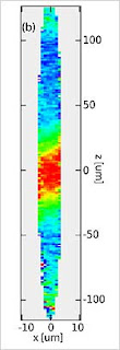
This photo of a Bose-Einstein condensate, only half a millimeter long and 10 microns wide, reveals minute variations in magnetic field across the sample. The ultra-cold gas of rubidium atoms can detect variations in magnetic field as small as one picoTesla, which is 50 million times smaller than Earth's magnetic field. (Stamper-Kurn lab/UC Berkeley)

This photo of a Bose-Einstein condensate, only half a millimeter long and 10 microns wide, reveals minute variations in magnetic field across the sample. The ultra-cold gas of rubidium atoms can detect variations in magnetic field as small as one picoTesla, which is 50 million times smaller than Earth's magnetic field. (Stamper-Kurn lab/UC Berkeley)
Physicists exploit ultra-cold gases to measure ultra-small magnetic fields

Berkeley -- Capturing the coldest atoms in the universe within the confines of a laser beam, University of California, Berkeley, physicists have made a device that can map magnetic fields more precisely than ever before.

Doctors now use sensitive magnetic field detectors called SQUIDS to record faint magnetic activity in the brain, while similar detectors are employed in fields ranging from geology to semiconductor manufacturing. One advantage of the new device, which is based on ultra-cold Bose Einstein condensates (BECs), is that it can measure low-frequency fields, such as slow brain waves, at a very high resolution and with very high sensitivity.

"This is not a bulk sensor for magnetic fields, but a precision magnetometer that can measure the magnetic field over small length scales, on the order of microns - a thousand times smaller than a millimeter - with a field sensitivity which is comparable to or better than modern scanning-SQUID microscopes," said Dan Stamper-Kurn, UC Berkeley associate professor of physics and faculty scientist at Lawrence Berkeley National Laboratory.

Stamper-Kurn and his colleagues, including postdoctoral researcher Mukund Vengalattore and former graduate student, now post-doc, James M. Higbie, reported their results in the May 18 issue of the journal Physical Review Letters.

The researchers created their device by cooling a gas of rubidium atoms (rubidium-87) to a mere 50 nanoKelvin - 50 billionths of a degree above absolute zero - to create a so-called spinor Bose-Einstein condensate. This is a quantum fluid that manifests both frictionless flow, making it a superfluid, and also magnetization, as a ferromagnet. By taking repeated pictures of the gas and exploiting its magnetic properties, they were able to detect, within a quarter-second measurement time, magnetic fields as small as 1 picoTesla, 50 million times weaker than the Earth's magnetic field of 50 microTesla.

What truly distinguishes this magnetic microscope, according to Stamper-Kurn, is not the smallness of the detected field, but rather the smallness of the spatial region in which this field was detected: an area only 10 microns by 10 micron, a millionth the area of a postage stamp.

For comparison, in mapping magnetic fields at similar spatial resolution, current devices such as SQUIDs (superconducting quantum interference devices) have, to date, reached sensitivities of only about 30 picoTesla over a one-second measurement time. At present, the BEC magnetometer matches, or even slightly improves upon, the theoretical limits to the sensitivity of a SQUID-based magnetic microscope, and further improvements beyond this limit appear possible, Stamper-Kurn said.
He predicts that, as the size and complexity of BEC-producing machines is reduced, BEC magnetometers could replace SQUID magnetometers in many applications, perhaps even for brain wave measurements, providing higher sensitivity at low frequencies and better spatial resolution.

Stamper-Kurn's laboratory focuses on studies and applications of BECs, which are gases so cold that all the atoms collapse into the same quantum state, becoming essentially indistinguishable from one another. Stamper-Kurn was a member of the Massachusetts Institute of Technology team that was among the first to create these supercold systems in 1995, a feat for which his advisor, physicist Wolfgang Ketterle, shared the 2001 Nobel Prize.

Though the first condensates were confined by magnetic fields to keep them from touching the walls of a container and heating up, Stamper-Kurn creates his within an "optical trap," essentially a low-power laser beam. He and his colleagues discovered that using an optical trap rather than a magnetic trap enabled the trapped atoms to respond to very minute magnetic fields. This is possible because, in a magnetic field, the spins of the atoms in a cold optical trap precess, just like the axis of a spinning top, at a frequency determined by the strength of the surrounding magnetic field.

A key element in the researchers' magnetometer is a method they developed for taking snapshot images of the orientation of the spin of the ultra-cold trapped gas. By taking a rapid-fire sequence of such snapshots, the team can record a movie of the spin of the atoms precessing, and then calculate the strength of the magnetic field from the rate of this precession. The point of using a BEC for such sensing is that the atoms in this quantum gas hardly move at all. Atoms at different locations can then be counted upon to sense only the magnetic field at their locale.

This feature provides the magnetic sensor with its impressive spatial resolution. Though some hot-gas systems, such as spin-polarized atomic gases, can be used to measure magnetic fields smaller than those measured using ultra-cold gases, their spatial sensitivity is worse because the hot gases diffuse quickly throughout the centimeter-sized devices. The laser-trapped BEC cloud is about one-half millimeter long and 10 microns across - about 10 percent the width of a human hair. One run of the magnetic sensor provides a map of the magnetic field across this entire area simultaneously.

"With the BEC's strengths - its stability, its long coherence times, the fact that collisions don't shift the precession frequency - we have all the ingredients we need for a high spatial resolution magnetometer," said Vengalattore.

"The fact that we can take a single picture showing how all the atomic 'compass needles' have been rotated by the local magnetic field is ideal for getting the precise information we need at once, without having to scan slowly over a surface," added Higbie.

"This finally delivers on the promise of using Bose-Einstein condensed atoms for precision measurement," said Stamper-Kurn.

Vengalattore admits that, for the foreseeable future, the magnetometer will be most useful in probing the magnetic properties of small physical systems like those under study in Stamper-Kurn's laboratory. Currently, the group is using this technique of imaging the spin of the atoms to study quantum phase transitions in a BEC. Just as water undergoes a thermal phase transition when the temperature rises, changing from ice to liquid, quantum systems undergo quantum phase transitions as conditions such as pressure and magnetic field change. The researchers aim to probe such quantum phase transitions using ultra-cold gases confined in a periodic potential called an optical lattice. By studying the magnetic properties of such model systems, they hope to better understand the behavior of more complex magnetic materials. ###

The work also was coauthored by UC Berkeley graduate students Sabrina R. Leslie, Jennie Guzman and Lorraine E. Sadler. The research was funded by the National Science Foundation and the David and Lucile Packard Foundation.

Contact: Robert Sanders rsanders@berkeley.edu 510-643-6998 University of California - Berkeley

Technorati Tags: or and or and or and or and or and or and or and or and

Wednesday, May 30, 2007

Inverse woodpile structure has extremely large photonic band gap

Paul Braun, a University Scholar and a professor of materials science and engineering, and Jennifer Lewis, the Thurnauer Professor of Materials Science and Engineering and interim director of the Frederick Seitz Materials Research Laboratory, Photo by L. Brian Stauffer

Books by the Authors by Paul V Braun Recommended by Jennifer A. Lewis "This book has been a valuable resource for my research group."

Polymeric Stabilization of Colloidal Dispersions (Colloid science)

Paul Braun, a University Scholar and a professor of materials science and engineering, and Jennifer Lewis, the Thurnauer Professor of Materials Science and Engineering and interim director of the Frederick Seitz Materials Research Laboratory, have created a germanium inverse woodpile structure that has one of the widest photonic band gaps ever reported.

To reach Paul Braun, call 217-244-7293; e-mail: pbraun@uiuc.edu.To reach Jennifer Lewis, call 217-244-4973; e-mail: jalewis@uiuc.edu.
CHAMPAIGN, Ill. — As many homeowners know, when stacking firewood, pieces should be placed close enough to permit passage of a mouse, but not of a cat chasing the mouse.

Now, imagine a woodpile where all those mouse passageways are packed with ice, the wood carefully removed, and you have an idea of what the latest photonic structure built by researchers at the University of Illinois looks like.

It’s called an inverse woodpile structure, and the U. of I. device is built of germanium, a material with a higher refractive index than silicon.

Until now, all woodpile structures have been composed of solid or hollow rods in an air matrix,” said Paul Braun, a University Scholar and a professor of materials science and engineering at the U. of I. “Our structure is composed of a germanium matrix containing a periodic array of tubular holes, made possible by a unique and flexible fabrication technique.”

In a paper accepted for publication in the journal Advanced Materials, and posted on its Web site, Braun and his co-authors describe the fabrication and optical properties of their germanium inverse woodpile structure; a structure with one of the widest photonic band gaps ever reported.

“A wider band gap means there is a broader spectral range where you can control the flow of light,” said Braun, who also is affiliated with the university’s Beckman Institute, Frederick Seitz Materials Research Laboratory, and Micro and Nanotechnology Laboratory. “In many applications, from low-threshold lasers to highly efficient solar cells, photonic crystals with wide band gaps may be required.”

To create their germanium inverse woodpile structure, the researchers first produced a polymer template by using a robotic deposition process called direct-write assembly.

The process employs a concentrated polymeric ink, dispensed as a filament to form the woodpile rods, from a nozzle approximately 1 micron in diameter (a micron is 1 millionth of a meter, approximately 50 times smaller than the diameter of a human hair).

The nozzle dispenses the ink into a reservoir on a computer-controlled, three-axis micropositioner. After the pattern for the first layer is generated, the nozzle is raised and another layer is deposited. This process is repeated until the desired three-dimensional structure is produced.

Next, the researchers deposited a sacrificial coating of aluminum oxide and silicon dioxide onto the entire structure. The coating enlarged the rods and increased the contact area between them. The space between the rods was subsequently filled with germanium.

The researchers then heated the structure to burn away the polymer template. Lastly, the sacrificial oxide coating was dissolved by acid, leaving behind a tiny block of germanium with an inner network of interconnected tubes and channels.
The finished structure – built and tested as a proof of concept – consists of 12 layers of tubes and measures approximately 0.5 millimeters by 0.5 millimeters, and approximately 15 microns thick.

“The direct-write template approach offers new design rules, which allows us to fabricate structures we otherwise could not have made,” said co-author Jennifer Lewis, the Thurnauer Professor of Materials Science and Engineering and interim director of the Frederick Seitz Materials Research Laboratory.

“Our technique also can be adopted for converting other polymeric woodpile templates, such as those made by laser-writing or electro-beam lithography, into inverse woodpile structures,” Lewis said.

In addition to their potential as photonic materials, the interconnected, inverse woodpile structures could find use as low-cost microelectromechanical systems, microfluidic networks for heat dissipation, and biological devices.

With Braun and Lewis, co-authors of the paper are postdoctoral research associate Florencio GarcĂ­a-Santamaria and graduate student Mingjie Xu, both at Illinois; electrical engineering professor Shanhui Fan at Stanford University; and physicist Virginie Lousse at the Laboratoire de Physique du Solide in Belgium.

The work was funded by the U.S. Department of Energy and the U.S. Army Research Office.

Contact: James E. Kloeppel kloeppel@uiuc.edu 217-244-1073 University of Illinois at Urbana-Champaign

Technorati Tags: or and or and or and or and or and or and or and or and

Tuesday, May 29, 2007

Nanoscale Pasta: Toward Nanoscale Electronics

Nanoscale Pasta: Toward Nanoscale Electronics

Transmission electron microscope (TEM) micrograph of a singly wound, coiled carbon nanofiber (NF) synthesized through thermal chemical vapor deposition (CVD),  at high In concentration (In/Fe ratio less than 3).San Diego, CA, May 17, 2007 – Pasta tastes like pasta – with or without a spiral. But when you jump to the nanoscale, everything changes: carbon nanotubes and nanofibers that look like nanoscale spiral pasta have completely different electronic properties than their non-spiraling cousins.
Engineers at UC San Diego, and Clemson University are studying these differences in the hopes of creating new kinds of components for nanoscale electronics.

We are looking at spiraling, bent and helical carbon nanotubes from the point of view of new functionality.
Can we get something totally different from these nonlinear nanotubes?” asked Prab Bandaru, a mechanical and aerospace engineering professor at the UC San Diego Jacobs School of Engineering.

For example, spiral shaped nanotubes could turn out to be important for new kinds of nanoscale switching and memory storage devices.
Prab Bandaru, professor of mechanical and aerospace engineering at UCSD
Recently, Bandaru won a National Science Foundation CAREER award for the study of nonlinear nanotubes. The Faculty Early Career Development (CAREER) Program is the NSF’s most prestigious award in support of the early career-development activities of junior faculty. Bandaru’s award carries with it a 5-year, $400,000 grant to support research aimed at developing new types of nanoelectronic components including electrical switches, logic elements, frequency mixers and nanoscale inductors.

Book By Dr. Apparao M. Rao Professor Department of Physics 202C Kinard Labs Clemson University Clemson, SC 29634Ph: (864) 656 – 6758 Email: arao@clemson.edu.
Such devices could some day outperform conventional silicon technologies on a number of levels, such as power consumption, radiation hardness, and heat dissipation.

Bandaru collaborates with Apparao Rao, of Clemson University, on the controlled synthesis of carbon nanotubes with a variety of shapes, including Y-junctions and nanohelices, through chemical vapor deposition processes. Once they are grown, transmission electron microscopy is used to perform structural analyses of the nonlinear nanotubes. The engineers are also investigating nanotube growth mechanisms, defects, nanoscale electrical conduction mechanisms and device modeling.In addition, they are exploring both the layout of electrical and optoelectronic circuits, and the limits of device operation through high frequency measurements.

“Because nanotubes are so small, you need to work at the atomic level to understand and manipulate them,” explained Bandaru. The presence or absence of single carbon atoms at strategic locations within nanotubes determines whether they have a linear or spiral shape.
Work on nonlinear nanowires is already well underway at UCSD and around the world. Bandaru, for example, is the first author on a paper recently published in the Journal of Applied Physics that outlines a mechanism for how carbon nanotubes and nanofibers grow.

In particular, the model predicts conditions under which coiling will happen. “Now that we know the exact conditions under which the helical nanostructures grow, we can exert greater control over the electronic and other properties of nonlinear nanotubes,” said Bandaru.
A mat of nanocoils. Scale bar = 2 micrometers
Exactly where, when and how linear and nonlinear nanotubes will make the leap from the laboratory to the real world is still unclear. Scientists have more to learn about their basic properties, about how to control their growth, and about how to integrate them into devices.

In August 2005, Bandaru made headlines around the world when his work on Y-shaped nanotubes appeared in the journal Nature Materials. Bandaru and colleagues at UCSD’s Jacobs School and Clemson University demonstrated that Y-shaped nanotubes can behave as electronic switches similar to conventional transistors, which are the workhorses of modern microprocessors, digital memory, and application-specific integrated circuits.

Nanotubes, of course, are not the only tiny spiraling structures. DNA and proteins also have helical structures. “It’s gratifying to encounter connections at the nanoscale between biological structures and helices and coils synthesized via chemical vapor deposition,” said Bandaru. “Our future work might improve our understanding of why helices abound in nature.”

Paper Reference: P.R. Bandaru et al, Journal of Applied Physics, vol. 101, no. 9, p 094307, 2007

Funders for research described in Journal of Applied Physics paper: The National Science Foundation and the Office of Naval Research.

The authors also appreciate the use of the facilities at the National Center for Electron Microscopy NCEM at the Lawrence Berkeley National Laboratory, Berkeley, CA.

Contact: Daniel Kane dbkane@ucsd.edu 858-534-3262 University of California - San Diego

Technorati Tags: or and or and or and or and or and or and or and or and

Monday, May 28, 2007

Iowa State scientists demonstrate first use of nanotechnology to enter plant cells

Iowa State scientists (from left) Brian Trewyn, Francois Torney, Kan Wang and Victor Lin are the first to use nanotechnology to penetrate rigid plant cell walls and deliver DNA and chemicals with precise control. Photo by Bob Elbert.AMES, Iowa -- A team of Iowa State University plant scientists and materials chemists have successfully used nanotechnology to penetrate plant cell walls and simultaneously deliver a gene and a chemical that triggers its expression with controlled precision.
Their breakthrough brings nanotechnology to plant biology and agricultural biotechnology, creating a powerful new tool for targeted delivery into plant cells.

The research, "Mesoporous Silica Nanoparticles Deliver DNA and Chemicals into Plants," is a highlighted article in the May issue of Nature Nanotechnology. The scientists are Kan Wang, professor of agronomy and director of the Center for Plant Transformation, Plant Sciences Institute; Victor Lin, professor of chemistry and senior scientist, U.S. Department of Energy's Ames Laboratory; Brian Trewyn, assistant scientist in chemistry; and Francois Torney, formerly a post-doctoral scientist in the Center for Plant Transformation and now a scientist with Biogemma, Clermond-Ferrand, France.

Currently, scientists can successfully introduce a gene into a plant cell. In a separate process, chemicals are used to activate the gene's function. The process is imprecise and the chemicals could be toxic to the plant.

"With the mesoporous nanoparticles, we can deliver two biogenic species at the same time," Wang said. "We can bring in a gene and induce it in a controlled manner at the same time and at the same location. That's never been done before."


The controlled release will improve the ability to study gene function in plants. And in the future, scientists could use the new technology to deliver imaging agents or chemicals inside cell walls. This would provide plant biologists with a window into intracellular events.

The Iowa State team, which has been working on the research in plants for less than three years, started with an Iowa State University proprietary technology developed previously by Lin's research group. It is a porous, silica nanoparticle system. Spherical in shape, the particles have arrays of independent porous channels. The channels form a honeycomb-like structure that can be filled with chemicals or molecules.

"One gram of this kind of material can have a total surface area of a football field, making it possible to carry a large payload," Trewyn said.

Lin's nanoparticle has a unique "capping" strategy that seals the chemical goods inside. In previous studies, his group successfully demonstrated that the caps can be chemically activated to pop open and release the cargo inside of animal cells. This unique feature provides total control for timing the delivery

The team's first attempt to use the porous silica nanoparticle to deliver DNA through the rigid wall of the plant cell was unsuccessful. The technology had worked more readily in animals cells because they don't have walls. The nanoparticles can enter animal cells through a process called endocytosis - the cell swallows or engulfs a molecule that is outside of it. The biologists attempted to mimic that process by removing the wall of the plant cell (called making protoplasts), forcing it to behave like an animal cell and swallow the nanoparticle. It didn't work.

They decided instead to modify the surface of the particle with a chemical coating.

"The team found a chemical we could use that made the nanoparticle look yummy to the plant cells so they would swallow the particles," Torney said.

It worked. The nanoparticles were swallowed by the plant protoplasts, which are a type of spherical plant cells without cell walls.

Most plant transformation, however, occurs with the use of a gene gun, not through endocytosis. In order to use the gene gun to introduce the nanoparticles to walled plant cells, the chemists made another clever modification on the particle surface. They synthesized even smaller gold particles to cap the nanoparticles. These "golden gates" not only prevented chemical leakage, but also added weight to the nanoparticles, enabling their delivery into the plant cell with the standard gene gun.

The biologists successfully used the technology to introduce DNA and chemicals to Arabidopsis, tobacco and corn plants.

"The most tremendous advantage is that you can deliver several things into a plant cell at the same time and release them whenever you want," Torney said.

"Until now, you were at nature's mercy when you delivered a gene into a cell," Lin said. "There's been no precise control as to whether the cells will actually incorporate the gene and express the consequent protein. With this technology, we may be able to control the whole sequence in the future."

And once you get inside the plant cell wall, it opens up "whole new possibilities," Wang said.

"We really don't know what's going on inside the cell. We're on the outside looking in. This gets us inside where we can study the biology per se," Wang said.

The interdisciplinary research collaboration was funded and facilitated by Iowa State's Plant Sciences Institute. The institute sponsors Wang's work to develop a male-sterile, biopharmaceutical corn - the corn contains a therapeutic protein but does not produce pollen. The materials development and synthesis of the nanoparticles in Lin's laboratory was funded by the energy department and the National Science Foundation. Wang and Lin intend to continue their collaboration to further develop the technology and its applications in plants. -30-

Contacts: Victor Lin, Chemistry, (515) 294-3135, vsylin@iastate.edu, Kan Wang, Center for Plant Transformation, (515) 294-4429, kanwang@iastate.edu, Francois Torney, Biogemma, (+33) 473 427 970, ftorney@gmail.com, Brian Trewyn, Chemistry, (515) 294-6220, bgtrewyn@iastate.edu, Teddi Barron, News Service, (515) 294-4778, tbarron@iastate.edu

Technorati Tags: or and or and or and or and or or and or and or and

Sunday, May 27, 2007

Inexpensive 'nanoglue' can bond nearly anything together

Caption: A new method allows a self-assembled molecular nanolayer to become a powerful nanoglue by 'hooking' together any two surfaces that normally don’t stick well. Unprotected, a nanolayer (green ball: silicon, blue: sulphur, red: carbon, white: hydrogen) would degrade or detach from a surface when heated to 400 degrees Celsius. But when topped with a thin copper film that binds strongly with the nanolayer, heat causes the nanolayer to form strong chemical bonds to the silica underlayer -- hooking or gluing the copper-silica 'sandwich' together. This technique produces a sevenfold increase of the thin film sandwich’s adhesion strength and allows the nanolayer to withstand temperatures of at least 700 degrees Celsius. Both features are unexpected and unprecedented. This new ability to bond together nearly any two surfaces using nanolayers will benefit nanoelectronics and computer chip manufacturing. Other envisioned applications include coatings for turbines and jet engines, and adhesives for high-heat environments. Credit: Rensselaer/G. Ramanath. Usage Restrictions: Please include credit line.Troy, N.Y. -- Researchers at Rensselaer Polytechnic Institute have developed a new method to bond materials that don’t normally stick together. The team’s adhesive, which is based on self-assembling nanoscale chains, could impact everything from next-generation computer chip manufacturing to energy production.
Less than a nanometer – or one billionth of a meter – thick, the nanoglue is inexpensive to make and can withstand temperatures far higher than what was previously envisioned. In fact, the adhesive’s molecular bonds strengthen when exposed to heat.

The glue material is already commercially available, but the research team’s method of treating the glue to dramatically enhance its “stickiness” and heat resistance is completely new. The project, led by Rensselaer materials science and engineering professor Ganapathiraman Ramanath, is featured in the May 17 issue of the journal Nature.

Like many key scientific discoveries, Ramanath and his team happened upon the novel, heat-hardened nanoglue by accident.
For years Ramanath has investigated ways of assembling layers of molecular chains between two different materials to enhance the structural integrity, efficiency, and reliability of semiconductor devices in computer chips. His team has shown that molecular chains with a carbon backbone – ending with appropriate elements such as silicon, oxygen, or sulfur – can improve adhesion and prevent heat-triggered mixing of atoms of the adjoining substances.Caption: A new method allows a self-assembled molecular nanolayer to become a powerful nanoglue by 'hooking' together any two surfaces that normally don’t stick well. Unprotected, a nanolayer (green ball: silicon, blue: sulphur, red: carbon, white: hydrogen) would degrade or detach from a surface when heated to 400 degrees Celsius. But when topped with a thin copper film that binds strongly with the nanolayer, heat causes the nanolayer to form strong chemical bonds to the silica underlayer -- hooking or gluing the copper-silica 'sandwich' together. This technique produces a sevenfold increase of the thin film sandwich’s adhesion strength and allows the nanolayer to withstand temperatures of at least 700 degrees Celsius. Both features are unexpected and unprecedented. This new ability to bond together nearly any two surfaces using nanolayers will benefit nanoelectronics and computer chip manufacturing. Other envisioned applications include coatings for turbines and jet engines, and adhesives for high-heat environments. Credit: Rensselaer/G. Ramanath. Usage Restrictions: Please include credit line.
Recently, Ramanath’s group and other researchers have found these nanolayers to be useful for creating adhesives, lubricants, and protective surface coatings.

The nanolayers, however, are extremely susceptible to heat and begin to degrade or simply detach from a surface when exposed to temperatures above 400 degrees Celsius. This severe limitation has precluded more widespread use of the nanolayers.

Ramanath’s team decided to sandwich a nanolayer between a thin film of copper and silica, thinking the extra support would help strengthen the nanolayer’s bonds and boost its adhesive properties. It proved to be an insightful venture, and the research team found more than it bargained for.

When exposed to heat, the middle layer of the “nanosandwich” did not break down or fall off – as it had nowhere to go. But that was not the only good news. The nanolayer’s bonds grew stronger and more adhesive when exposed to temperatures above 400 degrees Celsius. Constrained between the copper and silica, the nanolayer’s molecules hooked onto an adjoining surface with unexpectedly strong chemical bonds.

“The higher you heat it, the stronger the bonds are,” Ramanath said. “When we first started out, I had not imagined the molecules behaving this way.”

To make sure it wasn’t a fluke, his team recreated the test more than 50 times over the past two years. The results have been consistent, and show heating up the sandwiched nanolayer increases its interface toughness – or “stickiness” – by five to seven times. Similar toughness has been demonstrated using micrometer-thick layers, but never before with a nanometer-thick layer. A nanometer is 1,000 times smaller than a micrometer.

Because of their small size, these enhanced nanolayers will likely be useful as adhesives in a wide assortment of micro- and nanoelectronic devices where thicker adhesive layers just won’t fit.

Another unprecedented aspect of Ramanath’s discovery is that the sandwiched nanolayers continue to strengthen up to temperatures as high as 700 degrees Celsius. The ability of these adhesive nanolayers to withstand and grow stronger with heat could have novel industrial uses, such as holding paint on hot surfaces like the inside of a jet engine or a huge power plant turbine.

Along with nanoscale and high heat situations, Ramanath is confident the new nanoglue will have other unforeseen uses.

“This could be a versatile and inexpensive solution to connect any two materials that don’t bond well with each other,” Ramanath said. “Although the concept is not intuitive at first, it is simple, and could be implemented for a wide variety of potential commercial applications.

“The molecular glue is inexpensive – 100 grams cost about $35 – and already commercially available, which makes our method well-suited to today’s marketplace. Our method can definitely be scaled up to meet the low-cost demands of a large manufacturer,” he said.

Ramanath and his team have filed a disclosure on their findings and are moving forward toward a patent, which will complement the robust portfolio of other intellectual property they hold in this field. The team is also exploring what happens when certain variables of the nanoglue are tweaked, such as making taller nanolayers or sandwiching the layers between substances other than copper and silica.

Along with Ramanath, Rensselaer materials science and engineering graduate students Darshan Gandhi and Amit Singh contributed to the paper. Other co-authors include Rensselaer physics professor Saroj Nayak and graduate student Yu Zhou, IBM researcher Michael Lane at the T.J. Watson Research Center in Yorktown Heights, N.Y., and Ulrike Tisch and Moshe Eizenberg of the Technion-Israel Institute of Technology.

Ramanath’s ongoing research is supported by the National Science Foundation, the U.S.-Israel Binational Science Foundation, the Alexander von Humboldt Foundation, and New York state through the Interconnect Focus Center.

LaVerne Hess, the NSF program official most familiar with Ramanath’s work, applauded the interdisciplinary nature and strong technical relevance of the nanoglue project.

“It’s a good example of basic materials science research motivated by an understanding of engineering needs in the electronics field, and involving fundamental chemistry concepts to create new materials capabilities to enable progress in a field important to U.S. competitiveness,” Hess said. ###

News from Rensselaer Polytechnic InstituteMay 16, 2007 news.rpi.edu

Contact: Michael Mullaney mullam@rpi.edu 518-276-6161 Rensselaer Polytechnic Institute

About Rensselaer: Rensselaer Polytechnic Institute, founded in 1824, is the nation’s oldest technological university. The university offers bachelor’s, master’s, and doctoral degrees in engineering, the sciences, information technology, architecture, management, and the humanities and social sciences. Institute programs serve undergraduates, graduate students, and working professionals around the world.

Rensselaer faculty are known for pre-eminence in research conducted in a wide range of fields, with particular emphasis in biotechnology, nanotechnology, information technology, and the media arts and technology. The Institute is well known for its success in the transfer of technology from the laboratory to the marketplace so that new discoveries and inventions benefit human life, protect the environment, and strengthen economic development.

Technorati Tags: or and or and or and or and or or and or and or and

Saturday, May 26, 2007

microelectromechanical systems (MEMS) designs

MEMS student design contest winners announced by Sandia, Oklahoma and Illinois universities earn top micro design honors

An accordion? A road jack? Neither — it’s University of Oklahoma’s smallest-arm MEMS project, with out of plane extension capability and grabbers at far right.ALBUQUERQUE, N.M. — Two winners of the third annual University Alliance competition for student microelectromechanical systems (MEMS) designs have been announced by Sandia National Laboratories,
which originated and supports the competition High Resolution Image

The novel design category was won by a team from the University of Oklahoma, which wrested first place from perennial winner Texas Tech with a micro device impressively named Parvissimus bracchius, for “smallest arm.”

A second category, new this year, called for a micro design that would reliably inspect nanoscale phenomena. This was won by the University of Illinois at Urbana-Champaign (UIUC).
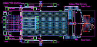
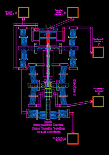
The UIUC tension-testing MEMS structure, utilizing a novel floating shuttle actuator, is intended to deform nano-objects so their physical properties can be measured.“This competition is an opportunity for universities around the country to participate in an experience that incorporates all the intricate details of design, analysis, and fabrication of complex MEMS devices,” says Mark Platzbecker, technical team lead in Sandia’s MEMS Core Technologies Dept. High Resolution Image. Sandia is a National Nuclear Security Administration laboratory.
The University of Oklahoma students, under the guidance of mechanical engineering Professor Harold Stalford, won for their design of a 3-D microstructure with a powered robotic “hand” at its summit.

“We wanted a 3-D structure with power and motion at the top,” student team leader Zach Butler explained to an audience of Sandia microdesigners. “We wanted a 3-D microrobot active above the chip and off the chip’s sides to grab theoretical microfruit off a low-hanging tree.”

The tool design shows a device with the ability to extend like an accordion or a micro automobile jack at the top.

The flat device, when heated, can rise one millimeter to a vertical position, with power available for actuators to perform tasks above the substrate through an extended arm reaching several hundred microns higher. Several tools for the extended arm are being investigated.

The device, said Butler, could make in vitro fertilization more efficient and provide less invasive biopsy procedures.

Kinematic simulations are in progress, he said.

In addition to Butler, other students on the team were Samuel Camp, Joseph Dingeldein, Andrew Mann, Stephen Thompson, and Andrea Watt.

The UIUC team was led by student Mohammad Naraghi under the direction of Professor Ioannis Chasiotis.

The UIUC device featured a mechanical testing platform capable of generating tens of micronewtons of force on highly deformable nanofibers, with a total displacement of 100 micrometers measurable by an integrated folded leaf spring-loaded cell.

Fabrication of the designs by winners and honorable-mention finishers are among the incentives offered by Sandia for schools to join and participate in the University Alliance. Each winning school also will receive a selection of their MEMS fabricated parts for use in their curriculum.

Seven participants in the Alliance, now 17 members strong, chose to enter this year’s competitions.

“The Sandia University Alliance is steadily growing,” said Tom Zipperian, Sandia senior manager for MESA microfabrication. “We expect to have 20 members by next year’s competition.”

For more information regarding the contest or becoming a member of the University Alliance, contact Stephanie Johnson at srjohns@sandia.gov

More contest information can be found at mems.sandia.gov/ua/contest

Sandia is a multiprogram laboratory operated by Sandia Corporation, a Lockheed Martin company, for the U.S. Department of Energy’s National Nuclear Security Administration. Sandia has major R&D responsibilities in national security, energy and environmental technologies, and economic competitiveness.

Sandia news media contact: Neal Singer, nsinger@sandia.gov, (505) 845-7078

Contact: Neal Singer nsinger@sandia.gov 505-845-7078 DOE/Sandia National Laboratories

Technorati Tags: or and or and or and or and or or and or and or and

Friday, May 25, 2007

How semiconducting nanowires grow and behave

Electrical Engineering Grad Student Racks Up Awards
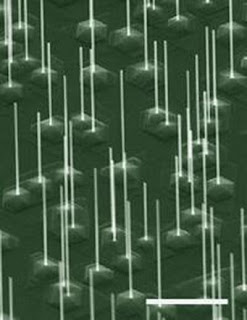
FE-SEM of InAs NWs grown by the VLS technique on InAs(111)B substrate. Scale bar is 2ÎĽm.San Diego, CA, May 14, 2007 -- For his work on how semiconducting nanowires grow and behave, Shadi A. Dayeh, a graduate student in the Department of Electrical and Computer Engineering (ECE) at the UCSD Jacobs School of Engineering, has recently earned a series of awards.
As LEDs, photovoltaics, biological and chemical sensors, nano-pipes for optical communications, and other applications, nanowires – crystalline fibers about one thousandth the width of a human hair – hold great promise. But there are many fundamental questions regarding how nanowires work and how they will perform in stressful, real-world conditions that need to be understood before nanowires get the chance to live up to the expectations. Shadi Dayeh, a Ph.D. candidate who works in the UCSD electrical engineering laboratories of both Deli Wang and Edward Yu, is deeply involved in this fundamental work on nanowires. Dayeh’s contributions are now being recognized by leaders in the field.
Schematic illustration of the Vapor-Liquid-Solid (VLS) nanowire growth mechanism.In March 2007, Dayeh learned that he won one of three best paper awards at the 2006 Electronic Materials Conference (EMC). Then, at the Materials Research Society (MRS) Spring meeting this April, Dayeh took home two more awards: the graduate student “silver medal” award
for his body of research on the synthesis and fabrication of compound semiconducting nanowires and devices for novel electronics; and a best poster award for research on field-, diameter-, and surface state- dependent transport behavior in semiconducting nanowires. In January 2007, Dayeh also received a Young Scientist Award at the 34th Conference on the Physics & Chemistry of Semiconductor Interfaces (PCSI-34).

In his award winning paper at EMC 2006, Dayeh helped to resolve a debate regarding which mechanism governs the growth of an important class of nanowires – the III-V compound semiconducting nanowires.
Dayeh and a team of electrical engineers from the Jacobs School demonstrated that the vapor-liquid-solid (VLS) growth mechanism that was proposed in 1964 does, in fact, extend to III-V compound semiconducting nanowires – a group that includes indium arsenide (InAs) nanowires.Shadi A. Dayeh, a graduate student in the Department of Electrical and Computer Engineering (ECE) at the UCSD Jacobs School of Engineering
This is noteworthy because, recently, researchers have claimed that III-V compound semiconducting nanowires grow via the vapor-solid-solid (VSS) growth mechanism.

“Shadi’s work not only improves our understanding of three-five nanowire growth, but it also opens the door to a wider tuning range of temperature and precursor flow rates to control nanowire growth rates, morphology, and material properties,” said Deli Wang.
The recent reports that the vapor-liquid-solid growth mechanism did not extend to III-V compound semiconducting nanowires left Dayeh unconvinced. After replicating the findings, he and the rest of the Jacobs School team tapped their understanding of the fundamental science of how nanowires grow and began experimenting.FE-SEM image of an InAs nanowire field effect transistor. Insets are the DC equivalent circuits with parasitic components.
“As the temperature increases, we know that the molar fraction of the group five element increases with respect to that of the group three element. This enhances thin-film growth and minimizes nanowire growth,” said Dayeh, who wondered if this could explain the reports that nanowire lengthening stopped when the growth temperature reached a certain critical value. This temperature was thought to be the melting temperature of the group III-Au alloy, typically employed in III-V compound nanowire growth.

Following this train of thought, Dayeh began tinkering with the initial molar ratios of the group III and group V precursor materials for InAs nanowires – tri-methyl-indium [In(CH3)3]and arsine [AsH3], respectively.

By starting with lower arsine concentrations, Dayeh demonstrated that III-V compound semiconducting nanowire growth prevails at higher temperatures according to the vapor-liquid-solid growth mechanism. He confirmed that the cessation of nanowire growth at certain high temperatures was tied to an imbalance in the molar ratios of the starting ingredients and not to a halted vapor-solid-solid growth mechanism.

Dayeh’s work on nanwires is broad in scope.

“My very recent work has shown that nanowires grown at different temperatures and in different crystallographic orientations exhibit notably different electronic properties,” said Dayeh.

In the work presented at the MRS 2007 spring meeting, Dayeh and colleagues at the Jacobs School performed a systemic study of carrier transport properties in InAs nanowire field effect transistors. This kind of research enables the understanding of important physical phenomena at the nanoscale and provides basic parameters for the design and fabrication of functional devices and integrated systems. The experimental studies include device scaling and miniaturization effects on performance as well as transport behavior and morphological changes when exposed to high applied electric fields. Among other implications, this line of research has highlighted thermal management as an important issue in realizing the full potential of nanowire-based devices

In work published online by the journal APPLIED PHYSICS LETTERS (selected by Virtual Journal of Nanoscale Science and Technology), Dayeh and a team of Jacobs School electrical engineers fabricated InAs nanowire field effect transistors (NWFETs) and investigated the capacitive effects of surface states on the field effect transistor (FET) transport properties. This analysis may help explain the wide range of nanowire parameters reported in the literature, which indicates that measurements at slow sweep rates enable a dynamic equilibrium of surface state charging and discharging and allow the extraction of the intrinsic nanowire transport parameters. This analysis also highlights the potential of InAs nanowires for high speed electronics with effective surface passivation.

In an earlier publication in the Journal of Vacuum Science and Technology B, Dayeh and Xiaotian Zhou, a graduate student in the UCSD materials science program who is advised by Edward Yu, observed room temperature ballistic transport in InAs nanowires over lengths up to ~200nm, another indication of the promise of this material.

“Shadi's studies of transport phenomena in InAs nanowires are helping to establish the foundation for the application of these materials in future high-performance electronic devices and circuits,” said Edward Yu.

In addition, the journal Small recently published research by Dayeh and colleagues at the Jacobs School demonstrating the promising potential of using InAs nanowires for high-speed nanoelectronics and providing analysis that enables accurate parameter extraction from such devices. In particular, the electrical engineers fabricated and characterized underlap top-gate and global back-gate InAs NWFETs, and demonstrated the highest semiconductor nanowire electron mobility reported to date.

“As a co-author on this paper, I experienced Shadi’s sharp intellect, creativity and sensitivity to detail. Shadi certainly exemplifies one of the great aspects of our ECE department. This is a place where students are challenged to solve some of the most pressing engineering questions of our time,” said Paul Yu, chair and professor, Department of Electrical and Computer Engineering, Jacobs School of Engineering .

Dayeh is also part of a broad collaboration of researchers at the Jacobs School that has recently reported breakthroughs in p-type ZnO nanowire synthesis and high sensitivity ZnO nanowire photodetectors, both published in Nano Letters and highlighted in the technology press.

Further information can be found at the Nano-Electronics, Photonics and Medicine and Nanoscale Characterization and Devices Laboratory websites.

Nano-Electronics, Photonics and Medicine (Deli Wang lab)
Nanoscale Characterization and Devices Laboratory (Edward Yu lab)

Funders: Office of Naval Research (ONR-Nanoelectronics), the National Science Foundation (NSF), Sharp Labs of America.

Dayeh and colleagues also recognize the staff of Calit2’s Nano3 Facility for maintenance of the nanofabrication environment.

Shadi Dayeh’s Recent Awards:

EMC 2006 best paper award: “Growth Mechanism and Optimization of InAs Nanowires Synthesized by OMVPE,” by Shadi A. Dayeh, David Aplin, Edward T. Yu, Paul K.L. Yu, and Deli Wang. All authors are from the Department of Electrical and Computer Engineering, UC San Diego Jacobs School of Engineering.

Spring MRS 2007 best poster award: “Field-, Diameter-, and Surface State- Dependent Transport Behavior in Semiconductor Nanowires,” by Shadi A. Dayeh, Paul K. L. Yu, Edward T. Yu, and Deli Wang. All authors are from the Department of Electrical and Computer Engineering, UC San Diego Jacobs School of Engineering.

Spring MRS 2007 Graduate Student Award: Silver Medal. PCSI-34 2007 Young Scientist Award.

Technorati Tags: or and or and or and or and or or and or and or and

Thursday, May 24, 2007

Berkeley Nanotechnology Pioneer to Receive $500,000 Waterman Award VIDEO

Annual prize from NSF recognizes outstanding young individual who is revolutionizing research

Peidong Yang, Waterman Awardee, Credit: National Science Foundation
The National Science Foundation (NSF) has chosen Peidong Yang, a chemist at the University of California, Berkeley, to receive the 2007 Alan T. Waterman Award. A nanotechnology expert, Yang has pioneered research on nanowires, strings of atoms that show promise for a range of high-technology devices, from tiny lasers and computer circuits to inexpensive solar panels and biological sensors.
Yang and his colleagues have grown arrays of zinc oxide and gallium nitride nanowires. Credit: Peidong Yang, University of California, BerkeleyThe annual Waterman award recognizes an outstanding young researcher in any field of science or engineering supported by NSF. Candidates may not be more than 35 years old, or 7 years beyond receiving a doctorate and must stand out for their individual achievements. In addition to a medal, the awardee receives a grant of $500,000 over a 3-year period for scientific research or advanced study in their field.
"Not only did Yang develop powerful methods to synthesize 1-dimensional semiconductor nanostructures, he continues to demonstrate such creative energy when exploring fundamental physical and chemical principles, such as the basic science needed to transform developments in fields ranging from sensors and molecular computers to biotechnology," said David Nelson, director of NSF's Solid-State Chemistry Program and one of the officers who has supported Yang's research.

In a relatively short time, Yang has created one of the nation's leading laboratories for the study of nanowires. Like nanotubes, nanowires are filaments only molecules wide with nearly miraculous properties, yet nanowires lack a hollow core and are proving generally easier to create and manipulate. Yang's research team has developed novel, efficient ways to create particularly sophisticated nanowires and complex nanowire arrays.
One of Peidong Yang's achievements was the development of a nanowire laser. Credit: Nicolle Rager Fuller, National Science Foundation"As we were dealing with a new class of nanostructure, naturally there were many fundamental questions and challenges that needed to be addressed," said Yang. "For example, how could we make them in a controlled manner? Do they have interesting chemical and physical properties? We are lucky that we are among the first few groups who started to address and answer some of these interesting questions."
By controlling the self-assembly of the wires and their orientation, Yang and his colleagues have created devices such as a wire only a hundred nanometers (billionths of a meter) wide that fires ultraviolet laser light; a patchwork of oriented nanowires that shows promise for shrinking the next generation of computer chips; and a nanowire array that has properties akin to solar panels but could potentially cost far less and is manufactured using an environmentally friendly process.

"Nanowires represent a rich family of functional materials," said Yang. "It is now possible to design and synthesize nanowires with quite complex structures based on progress made in the past couple of years. This type of control in nanostructural engineering has generated a rich collection of fascinating properties and functionalities, including nanoscale lasers, nanowire-based transistors, sensors and solar cells. These nanowire materials will have a particularly significant impact in areas such as energy conversion and solid state lighting."

Peidong Yang was born and raised in the Chinese city of Suzhou, leaving to study chemistry at the University of science and Technology of China in Hefei in 1988. Earning his Ph.D. degeree from Harvard in 1997, Yang then traveled to UC, Santa Barbara in 1997, and arrived at UC-Berkeley in 1999. In a short time, Yang has established himself as a rising star, publishing widely and receiving such awards as the NSF Young Investigator Award, the Alfred P. Sloan research fellowship, the Arnold and Mabel Beckman Young Investigator Award, the MRS Young Investigator Award, the Julius Springer Prize for Applied Physics, and the American Chemical Society's Pure Chemistry Award.

Following the award ceremony at the U.S. State Department on May 14th, NSF will host Yang and a distinguished panel on May 15th in a teleconference for journalists on emerging nanotechnologies. The program will highlight laboratory developments poised to become marketable products in the future. Information is available in the On the Nano Horizon: Emerging Technologies media advisory.

In addition to his Waterman award, Yang has received support from NSF through grants 0352750 and 0092086, as head graduate advisor for the Graduate Group in Nanoscale Science and Engineering through NSF IGERT grant 0333455 and as co-principal investigator for the NSF Center of Integrated Nanomechanical Systems, a Nanoscale Science and Engineering Center. -NSF-

Peidong Yang Department of ChemistryDepartment of Materials Science and EngineeringUniversity of California, Berkeley(510) 643-1545 cchem.berkeley.edu/~pdygrp/

Peidong Yang received a B.S. in chemistry from the University of Science and Technology of China in 1993 and a Ph.D. in chemistry from Harvard University in 1997. Following postdoctoral research at the University of California, Santa Barbara, Yang joined the faculty in the department of Chemistry at the University of California, Berkeley in 1999.

Currently associate professor in the Department of Chemistry, Materials Science and Engineering, he is also the deputy director for the Center of Integrated Nanomechanical Systems. Yang also serves as an associate editor for the Journal of the American Chemical Society (ACS).

In addition to the 2007 NSF Waterman Award, Yang has received the NSF CAREER Award, the Alfred P. Sloan research fellowship, the Arnold and Mabel Beckman Young Investigator Award, the MRS Young Investigator Award, the Julius Springer Prize for Applied Physics, and the ACS Pure Chemistry Award. Yang's main research interests focus on one-dimensional semiconductor nanostructures and their applications in nanophotonics, nanoelectronics, energy conversion and nanofluidics.

Contact: Josh Chamot jchamot@nsf.gov 703-292-7730 National Science Foundation

Program Contacts Jimmy Hsia, NSF (703) 292-7020 jhsia@nsf.gov David L. Nelson, NSF (703) 292-4932 dnelson@nsf.gov Mayra N. Montrose, NSF (703) 292-4757 mmontros@nsf.gov

Principal Investigators Peidong Yang, University of California, Berkeley (510) 643-1545 p_yang@uclink.berkeley.edu

Related WebsitesFact Sheet: Alan T. Waterman Award: nsf.gov/news/news_summ

The National Science Foundation (NSF) is an independent federal agency that supports fundamental research and education across all fields of science and engineering, with an annual budget of $5.91 billion. NSF funds reach all 50 states through grants to nearly 1,700 universities and institutions. Each year, NSF receives about 40,000 competitive requests for funding, and makes nearly 10,000 new funding awards. The NSF also awards over $400 million in professional and service contracts yearly.

Technorati Tags: or and or and or and or and or or and or and or and

Wednesday, May 23, 2007

DNA sieve -- Nanoscale pores can be tiny analysis labs

Caption: Graphic showing a lipid bilayer membrane (blue) with an alpha-hemolysin nanopore. A polyethylene glycol molecule (green globular structure) is transiting the pore; others are in solution on one side of the membrane. The colored spheres represent individual atoms, and are approximately 0.5 nanometers in diameter, or one twenty-thousandth the width of a human hair. Credit: NIST, Usage Restrictions: None.Imagine being able to rapidly identify tiny biological molecules such as DNA and toxins using less than a drop of salt water in a system that can fit on a microchip. It's closer than you might believe, say a team of researchers at the National Institute of Standards and Technology (NIST), Brazil's Universidade Federal de Pernambuco, and Wright State University in Dayton, Ohio.
In a paper appearing next week in the Proceedings of the National Academy of Sciences,* the team proves for the first time that a single nanometer-scale pore in a thin membrane can be used to accurately detect and sort different-sized polymer chains (a model for biomolecules) that pass through or block the channel.

Traditionally, unknown molecules are measured and identified using mass spectrometry, a process that involves ionizing and disintegrating large numbers of a target molecule, then analyzing the masses of the resulting molecules to produce a "molecular fingerprint" for the original sample. This equipment can cover a good-sized desk. By contrast, the "single-molecule mass spectrometry" system described in the PNAS paper is a non-destructive technique that in principle can measure one molecule at a time in a space small enough to fit on a single microchip device.

The technique involves creating a lipid bilayer membrane similar to those in living cells, and "drilling" a pore in it with a protein (alpha-hemolysin) produced by the Staphyloccoccus aureus bacteria specifically to penetrate cell membranes. Charged molecules (such as single-stranded DNA) are forced one-at-a-time into the nanopore, which is only 1.5 nanometers (the diameter of a human hair is about 10,000 nanometers) at its smallest point, by an applied electric current. As the molecules pass through the channel, the current flow is reduced in proportion to the size of each individual chain, allowing its mass to be easily derived.

In this experiment, various-sized chains in solution of the uncharged polymer polyethylene glycol (PEG) were substituted for biomolecules. Each type of PEG molecule reduced the nanopore's electrical conductance differently as it moved through, allowing the researchers to distinguish one size of PEG chain from another.

As a control, a solution of a highly purified PEG of a specific size was characterized with the nanopore. The resulting "fingerprint" closely matched the one identifying samples of the same size polymer in the mixed chain solution.

Further enhancement of the data from both the experimental and control tests yielded mass measurements and identifications of the different PEG chains that correlate with those made by traditional mass spectrometry.

Because the dimensions of the lipid bilayer and the alpha-hemolysin pore, as well as the required amount of electrical current, are at the nanoscale level, the "single-molecule mass spectrometry" technology may one day be incorporated into "lab-on-a-chip" molecular analyzers and single-strand DNA sequencers. ###

* J.W.F. Robertson, C.G. Rodriguez, V.M. Stanford, K.A. Rubinson, O.V. Krasilnikov and J.J. Kasianowicz. Single-moelcule mass spectrometry in solution using a solitary nanopore. Proceedings of the National Academy of Sciences 104 (20): 8207, May 15, 2007.

Contact: Michael E. Newman michael.newman@nist.gov 301-975-3025 National Institute of Standards and Technology (NIST)

Technorati Tags: or and or and or and or and or or and or and or and

Tuesday, May 22, 2007

Wetter report: New approach to testing surface adhesion

Caption: Wetability gradient: Water sprayed on a glass slide coated with a nanostructured gradient wettability film using the new NIST technique illustrates the transition from (A) superhydrophobicity to (C) superhydrophilicity. The lower image shows the magnified image of the (A) hydrophobic to (B) transition wetting region. The pink dotted line indicates the border of the superhydrophobic region, and the yellow dotted region shows a hydrophobic 'sticky' region. Credit: NIST, Usage Restrictions: NoneWith a nod to one of nature's best surface chemists—an obscure desert beetle—polymer scientists at the National Institute of Standards and Technology (NIST) have devised a convenient way to construct test surfaces with a variable affinity for water,
so that the same surface can range from superhydrophilic to superhydrophobic, and everything in between. Their technique, reported in a recent issue of the journal Langmuir,* may be used for rapid evaluation of paints and other materials that need to stick to surfaces.

The NIST team developed a flexible technique, based on ultraviolet light and photosensitive materials, to mimic one of nature's cleverest feats of surface chemistry. The Stenocara beetle of Africa's Namib Desert is able to thrive in a habitat so parched that not even the morning fog will condense. All the beetle has to do is raise its warty-looking wing covers into the breeze. Because the bumps are hydrophilic, or water-attracting, while the rest of the surface is hydrophobic, or water-repelling, the few water molecules that do strike the wing covers tend to get pushed uphill and collect on the bumps—where they eventually condense into artificial dewdrops that roll into the insect's mouth. The insect's trick is to use both surface structure and chemistry to create a surface that shifts rapidly from hydrophobic to hydrophilic.

The NIST researchers begin by coating the surface with a matrix of silica granules about 11 nanometers across. As with the beetle, whose wing covers are coated with organic particles about a thousand times larger, the spacing of the matrix provides a first, purely physical level of control over wettability: a water droplet placed atop the granules can sag only just so far into the gaps before it is stopped by surface tension.

The researchers then add a second level of control by coating the granules with a compound that changes their water affinity, in much the same way that a waxy substance makes some of the beetle's microparticles hydrophobic. This step in itself is not unique; other research groups have added such compounds to granular surfaces using electrochemical techniques. The NIST group's innovation is to use an optical technique that is much easier to modulate, and that can be carried out in air. They simply coat the granules with a photosensitive material, and expose it to ultraviolet light: the longer and more intense the exposure in a given area, the more hydrophilic that area becomes.

The new technique's most immediate application is for testing paints, adhesives and other coatings: instead of daubing the compounds on dozens of surfaces one by one, researchers can now spread them over a single surface that tests the entire range of wettability within the space of a few centimeters. Other applications also are possible, ranging from water collection in dry regions to open-air microchannel devices. Indeed, the same technique can be used to create surfaces that vary in their affinity for alcohol and many other small molecule liquids. ###

* J.T. Han, S. Kim and A. Karim. UVO-tunable superhydrophobic to superhydrophilic wetting transition on biomimetic nanostructured surfaces. Langmuir 2007, 23, 2608-2614.

Contact: Michael E. Newman michael.newman@nist.gov 301-975-3025 National Institute of Standards and Technology (NIST)

Technorati Tags: or and or and or and or and or or and or and or and

Monday, May 21, 2007

Tiny spectrometer offers precision laser calibration

Caption: Photographed adjacent to an ordinary green pea, NIST's microfabricated spectrometer consists of a tiny container of atoms, a photodetector and miniature optics. Credit: Svenja Knappe/NIST, Usage Restrictions: NoneA tiny device for calibrating or stabilizing precision lasers has been designed and demonstrated at the National Institute of Standards and Technology (NIST). The prototype device could replace table-top-sized instruments used for laser calibration in atomic physics research,
could better stabilize optical telecommunications channels, and perhaps could replace and improve on the precision of instrumentation used to measure length, chemicals or atmospheric gases.

The new spectrometer, described in the May 7 issue of Optics Express,* is the latest in a NIST series of miniaturized optical instruments such as chip-scale atomic clocks and magnetometers. The spectrometer is about the size of a green pea and consists of miniature optics, a microfabricated container for atoms in a gas, heaters and a photodetector, all within a cube about 10 millimeters on a side. The package could be used to calibrate laser instruments, or, if a miniature laser were included in the device, could serve as a wavelength or frequency reference.

Most of the optical components are commercially available. The key to the device is a tiny glass-and-silicon container—designed and fabricated at NIST—that holds a small sample of atoms. The sample chambers were micromachined in a clean room and filled and sealed inside a vacuum to ensure the purity of the atomic gas, but they can be mass-produced from silicon wafers into much smaller sizes, requiring less power and potentially cheaper than the traditional blown-glass containers used in laboratories. Although shrinking container size creates some limitations, NIST scientists have accommodated these difficulties by adding special features, such as heaters to keep more atoms in the gas state. NIST tests predict that the stability and signal performance of the tiny, portable device can be comparable to standard table-top setups.

The instrument works by measuring the intensity of a laser beam after it interacts with the atoms. The amount of light absorbed at a particular wavelength produces a characteristic signature. NIST has demonstrated the spectrometer with rubidium and cesium atoms, which absorb light at infrared, near-visible wavelengths, commonly used in atomic physics research. Different atoms or molecules, such as potassium or iodine, could be used for different applications. Or, a waveguide could be added to the device to double the frequency to stabilize lasers used in fiber-optic telecommunications. The mini-spectrometer would offer greater precision than the physical references now used to separate fiber-optic channels, with the advantage that more channels might be packed into the same spectrum. ###

* S.A. Knappe, H.G. Robinson and L. Hollberg. Microfabricated saturated absorption laser spectrometer. Optics Express. May 7, 2007.

Contact: Laura Ost laura.ost@nist.gov 303-497-4880 National Institute of Standards and Technology (NIST)

Technorati Tags: or and or and or and or and or or and or and or and