Wednesday, November 29, 2006

Have yourself a merry 'nano' Christmas!

Have yourself a merry 'nano' Christmas! Nanotechnology holiday gifts

350TC Nano-Tex Sheet Set by StudioWASHINGTON -- Tell a friend you are buying them a nanotechnology gift for the holidays, and visions of Star Trek collectables or geeky electronic toys start to dance in their heads. Nanotechnology Consumer Products
But nanotechnology gifts can include everything from fleece jackets and gloves from the Lands’ End™ catalogue—with Nano-Tex® Resists Static treatment—to an Apollo Diamond® engagement ring.

For do-it-yourselfers, there are Black & Decker’s DeWalt cordless power tools, with a powerful nanotech battery. Children wish for Apple’s® iPod Nano®. Twentysomethings may think the ideal present for their first apartment kitchen is a set of FresherLonger™ Miracle Food Storage containers by Sharper Image®, infused with naturally antibacterial silver nanoparticles which makers claim help fruits, vegetables, cheeses and even raspberries stay fresh longer. Or, they may want the Babolat® NS™ Tour Tennis Racket, with carbon nanotubes used to stiffen key areas of the racquet head and shaft, which the company touts as 100 times more rigid than steel and 6 times lighter!

According to recent polls, the majority of Americans have heard little or nothing about nanotechnology. But last year, according to Lux Research, nanotechnology was incorporated into more than $30 billion in manufactured goods. By 2014, an estimated $2.6 trillion in global manufactured goods will incorporate nanotechnology.

This first and largest publicly available inventory of nanotechnology consumer products is newly updated with almost 70 percent more nanotechnology consumer products than when it was first launched in March 2006. Nanoscale silver is now the most often identified nanomaterial used in consumer products in the inventory. The number of products containing nano-engineered silver has nearly doubled in eight months. The second highest nanoscale material cited by manufacturers is carbon, including carbon nanotubes and fullerenes, up almost 35 percent.

Nanotechnology is the ability to measure, see, manipulate and manufacture things usually between 1 and 100 nanometers (nm). A nanometer is one billionth of a meter. A human hair is roughly 100,000 nanometers wide. The limit of the human eye’s capacity to see without a microscope is about 10,000 nm. ###

The Project on Emerging Nanotechnologies is an initiative launched by the Woodrow Wilson International Center for Scholars and The Pew Charitable Trusts in 2005. It is dedicated to helping business, government and the public anticipate and manage possible health and environmental implications of nanotechnology.

Contact: Sharon McCarter sharon.mccarter@wilsoncenter.org 202-691-4016 Project on Emerging Nanotechnologies

Technorati Tags: or and or and or and or and or and or and or and or

Wednesday, November 22, 2006

A quantum (computer) step

Caption: University of Utah physicist Christoph Boehme works with equipment that he uses to show it it feasible for a superfast quantum computer of the future to read data that is stored in the form of magnetic 'spins' of phosphorus atoms. Credit: John Lupton, University of Utah, Usage Restrictions: NoneStudy shows it's feasible to read data stored as nuclear 'spins'. A University of Utah physicist took a step toward developing a superfast computer based on the weird reality of quantum physics
by showing it is feasible to read data stored in the form of the magnetic "spins" of phosphorus atoms.

"Our work represents a breakthrough in the search for a nanoscopic [atomic scale] mechanism that could be used for a data readout device," says Christoph Boehme, assistant professor of physics at the University of Utah. "We have demonstrated experimentally that the nuclear spin orientation of phosphorus atoms embedded in silicon can be measured by very subtle electric currents passing through the phosphorus atoms."

The study by Boehme and colleagues in Germany will be published in the December issue of the journal Nature Physics and released online Sunday, Nov. 19.

"We have resolved a major obstacle for building a particular kind of quantum computer, the phosphorus-and-silicon quantum computer," says Boehme. "For this concept, data readout is the biggest issue, and we have shown a new way to read data."

Boehme, who joined the University of Utah faculty earlier this year, conducted the study with Klaus Lips – a former colleague at the Hahn-Meitner Institute in Berlin – and with graduate students Andre Stegner and Hans Huebl and physicists Martin Stutzmann and Martin S. Brandt of the Technical University of Munich.

A Bit about Quantum Computing

In modern digital computers, information is transmitted by flowing electricity in the form of electrons, which are negatively charged subatomic particles. Transistors in computers are electrical switches that store data as "bits," in which "off" (no electrical charge) and "on" (charge is present) represent one bit of information: either 0 or 1.

For example, with three bits, there are eight possible combinations of 1 or 0: 1-1-1, 0-1-1, 1-0-1, 1-1-0, 0-0-0, 1-0-0, 0-1-0 and 0-0-1. But three bits in a digital computer can store only one of those eight combinations at a time.

Quantum computers, which have not been built yet, would be based on the strange principles of quantum mechanics, in which the smallest particles of light and matter can be in different places at the same time.

In a quantum computer, one "qubit" – quantum bit – could be both 0 and 1 at the same time. So with three qubits of data, a quantum computer could store all eight combinations of 0 and 1 simultaneously. That means a three-qubit quantum computer could calculate eight times faster than a three-bit digital computer.

Typical personal computers today calculate 64 bits of data at a time. A quantum computer with 64 qubits would be 2 to the 64th power faster, or about 18 billion billion times faster. (Note: billion billion is correct.)

Researchers are exploring many approaches to storing and processing information in nanoscopic form – on the scale of molecules and atoms, or one billionth of a meter in size – for quantum computing. They include optical quantum computers that would hold data in the form of on-off switches made of light, ions (electrically charged atoms), the size or energy state of an electron's orbit around an atom, so-called "quantum dots" of material and the "spins" or magnetic orientation of the centers or nuclei of atoms.

A New Spin on Quantum Computers

Boehme's new study deals with an approach to a quantum computer proposed in 1998 by Australian physicist Bruce Kane in a Nature paper titled "A silicon-based nuclear spin quantum computer." In such a computer, silicon – the semiconductor used in digital computer chips – would be "doped" with atoms of phosphorus, and data would be encoded in the "spins" of those atoms' nuclei. Externally applied electric fields would be used to read and process the data stored as "spins."

Spin is difficult to explain. A simplified way to describe spin is to imagine that each particle – like an electron or proton in an atom – contains a tiny bar magnet, like a compass needle, that points either up or down to represent the particle's spin. Down and up can represent 0 and 1 in a spin-based quantum computer, in which one qubit could have a value of 0 and 1 simultaneously.

In the new study, Boehme and colleagues used silicon doped with phosphorus atoms. By applying an external electrical current, they were able to "read" the net spin of 10,000 of the electrons and nuclei of phosphorus atoms near the surface of the silicon.

A real quantum computer would need to read the spins of single particles, not thousands of them. But previous efforts, which used a technique called magnetic resonance, were able to read only the net spins of the electrons of 10 billion phosphorus atoms combined, so the new study represents a million-fold improvement and shows it is feasible to read single spins – something that would take another 10,000-fold improvement, Boehme says.

But the point of the study, he adds, is that it demonstrates it is possible to use electrical methods to detect or "read" data stored as not only electron spins but as the more stable spins of atomic nuclei.

"We discovered a mechanism that will allow us to measure the spins of the nuclei of individual phosphorus atoms in a piece of silicon when the phosphorus is close [within about 50 atoms] to the surface," Boehme says. With improved design, it should be possible to build a much smaller device that "lets us read a single phosphorus nucleus."

Details of the Experiment

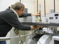
The researchers used a piece of silicon crystal about 300 microns thick – about three times the width of a human hair – less than 3 inches long and about one-tenth of an inch wide. The silicon crystal was doped with phosphorus atoms. Phosphorus atoms were embedded in silicon because too many phosphorus atoms too close together would interact with each other so much that they couldn't store information. The concept is that the nuclear spin from one atom of phosphorus would store one qubit of information.

The scientists used lithography to print two gold electrical contacts onto the doped silicon. Then they placed an extremely thin layer of silicon dioxide – about two billionths of a meter thick – onto the silicon between the gold contacts. As a result, the device's surface had tiny spots where the spins of phosphorus atoms could be detected.

The scientists applied a tiny voltage to the gold contacts, creating an electrical current perhaps 10,000 times smaller than that produced by an AA-size battery, Boehme says. When the current was measured during 100 millionths of a second, it stayed constant, indicating the spins of the phosphorus atoms in the silicon were random, with half pointing up and half pointing down.

Then the device was chilled with liquid helium to 452 degrees below zero Fahrenheit. That made most of the phosphorus spins point down. Next, the researchers applied a magnetic field and microwave radiation to the sample, which makes the phosphorus spins constantly flop up and down in concert for a few billionths of a second.

As a result, the electrical current fluctuated up and down.

"That is basically a readout of phosphorus electron spins," which, in turn, also can be used to determine the spins of the phosphorus atoms' nuclei based on a previously known relationship between electron spins and nuclear spins, Boehme says.

While Boehme is excited by this advance, numerous obstacles remain before quantum computing becomes a reality.

"If you want to compare the development of quantum computers with classical computers, we probably would be just before the discovery of the abacus," he says. "We are very early in development." ###

Embargoed by the journal Nature Physics for release at 11 a.m. MST Sunday, Nov. 19, 2006

Contact: Christoph Boehme boehme@physics.utah.edu 801-859-7896 (cellular) 801-581-6806 (office) 801-581-6992 (lab)

Lee Siegel leesiegel@ucomm.utah.edu 801-244-5399 (cellular) 801-581-8993 (office) University of Utah

University of Utah Public Relations 201 Presidents Circle, Room 308 Salt Lake City, Utah 84112-9017 (801) 581-6773 fax: 585-3350 unews.utah.edu

Technorati Tags: or and or and or and or and or and or and or and or

Thursday, November 16, 2006

Nanotech tools yield DNA transcription breakthrough

Credit: Image provided by Achillefs Kapanidis, Shimon Weiss, and Richard H. Ebright. Usage Restrictions: None.Caption: Initial transcription by RNA polymerase proceeds through a "DNA scrunching" mechanism, in which the enzyme remains stationary on promoter DNA and pulls into itself downstream DNA.
[Proposed movements of the template and nontemplate DNA strands are indicated by blue outlined and red-outlined arrows. Proposed positions at which the scrunched template and nontemplate DNA strands emerge from the enzyme are indicated by orange and pink dashed lines.

Positions of fluorescent probes used to analyze scrunching are indicated in green (donor probe on polymerase), brick red (acceptor probe at promoter position +20 in absence of scrunching), and bright red (acceptor probe at promoter position +20 in presence of scrunching).]

NEW BRUNSWICK/PISCATAWAY, N.J. -- Rutgers researcher Richard H. Ebright and his collaborators have resolved key questions regarding transcription, the fundamental life process that was the subject of the 2006 Nobel Prize in Chemistry.

Transcription is the first step in the process cells employ to read and carry out the out instructions contained in genes. Transcription is carried out by a molecular machine known as RNA polymerase, which synthesizes an RNA copy of the information in DNA.

Two papers by Ebright and collaborators in the Nov. 17 issue of the journal Science define for the first time the mechanisms by which the machine begins synthesis of RNA and then breaks free from its initial binding site to move along DNA to continue synthesizing RNA.

The results establish that during transcription initiation the machine remains stationary at its initial binding site and "reels in" adjacent DNA segments, unwinding these segments and pulling the unwound DNA strands into itself. This remarkable mechanism, termed "DNA scrunching," enables the machine to acquire and accumulate the energy it needs to break its binding interactions with the initial binding site, and to begin to move down the gene.

"Our findings were made possible by newly developed, single-molecule methods," said Ebright, a Howard Hughes Medical Institute investigator and professor of chemistry and chemical biology at Rutgers, The State University of New Jersey. "These methods enabled us to analyze and manipulate individual molecules of the machine, one-by-one, as they carried out reactions."

The discoveries significantly advance our understanding of the structure and function of the molecular machine that carries out transcription, setting the stage for new opportunities in combating the bacterial diseases that kill 13 million persons each year worldwide.

"For six decades, antibiotics have been our bulwark against bacterial infectious diseases, but this bulwark now is collapsing," said Ebright. "For all major bacterial pathogens, including tuberculosis, strains such as XDR-TB that are resistant to current antibiotics have emerged."

In addition, bacterial pathogens that may be used in bioterrorism can be engineered, and, in the former Soviet Union, were intentionally engineered to be resistant to current antibiotics.

Ebright explained that his laboratory at Rutgers' Waksman Institute of Microbiology has two parts: One part seeks a fundamental understanding of the machine; the other uses that understanding to develop new classes of antibacterial agents that function by inhibiting the bacterial version of the machine. "There is a direct information flow from our basic research to our applied research," he said. "Our basic research identifies new vulnerabilities within the bacterial version of the machine; our applied research exploits those vulnerabilities."

One of the studies reported in Science was conducted by Ebright's laboratory in conjunction with Shimon Weiss' laboratory at the California NanoSystems Institute of the University of California-Los Angeles (UCLA). The study by the Rutgers/UCLA team used single-molecule fluorescence spectroscopy. The researchers attached pairs of fluorescent "tags" to key structural elements of the machine and then monitored changes in distance between tags in single molecules as transcription occurred. The researchers showed that, during initial transcription, the machine does not move to reach adjacent DNA segments; nor does it stretch to reach adjacent DNA segments (as had been proposed two decades ago in models termed "transient excursions" and "inchworming"). Instead, the researchers showed that the machine remains stationary and pulls adjacent DNA segments into itself.

"The study of molecular machines and the dynamics of their moving parts hold great interest for nanotechnologists," said Weiss, leader of the UCLA group. "Beyond furthering the understanding of transcription, the novel methods and findings of this work will aid future studies of other molecular machines involved in cell replication, transcription and protein synthesis."

The other study reported in Science was conducted by Ebright's laboratory in collaboration with Terence Strick's laboratory at the Institut Jacques Monod in Paris. The study by the Rutgers/Paris team used single-molecule nanomanipulation. The researchers used an instrument referred to as "magnetic tweezers" to hold, stretch and twist a single molecule of DNA having a single start site for transcription. They then read out changes in the conformation of the DNA molecule in real time as transcription occurred. The researchers showed that the molecular machine responsible for transcription unwinds adjacent DNA segments and pulls unwound DNA into itself during initial transcription ("scrunching").

In addition, the researchers showed that machine rewinds this unwound DNA when the machine leaves the start site and begins to move down the gene ("unscrunching"). Finally, the researchers showed that this process of scrunching and unscrunching occurs every time that transcription initiation occurs, indicating that the process is an obligatory part of transcription initiation.

Taken together, the two studies answer the longstanding question of how the machine acquires the energy required to break its interactions with, and leave, the start site. The machine acquires this energy by unwinding DNA and pulling unwound DNA during initial transcription. As DNA is unwound, energy is stored in the system, in the same manner, Ebright notes, as winding the rubber band of a rubber-band-powered airplane stores energy. Eventually, there is sufficient energy stored in the system that the machine is able to break its interactions with the start site, to shoot forward and, at the same instant, to rewind the unwound DNA.

Ebright stated that the publication of these findings is part of a long-term collaboration with the UCLA and the Institut Jacques Monod groups. "Our ties are close," he said. "Three former Rutgers graduate students have gone on from my lab to the Weiss lab, and two other Rutgers graduate students have worked in the Strick lab during their thesis studies."

###, 061113-1 EbrightRNAP.rev.ed

Contact: Joseph Blumberg blumberg@ur.rutgers.edu 732-932-7084 x652 Rutgers, the State University of New Jersey

Technorati Tags: or and or and or and or and or and or and or and or

Sunday, November 12, 2006

'Nanorust' cleans arsenic from drinking water.

'Nanorust' cleans arsenic from drinking water, Tiny tech promises 'no-energy' solution for global problem.

Caption: This image depicts nanoparticles of rust in water. Credit: CBEN/Rice University, Usage Restrictions: None.HOUSTON, Nov. 9, 2006 -- The discovery of unexpected magnetic interactions between ultrasmall specks of rust is leading scientists at Rice University's Center for Biological and Environmental Nanotechnology (CBEN),
to develop a revolutionary, low-cost technology for cleaning arsenic from drinking water. The technology holds promise for millions of people in India, Bangladesh and other developing countries where thousands of cases of arsenic poisoning each year are linked to poisoned wells.

The new technique is described in the Nov. 10 issue of Science magazine.
Caption: Rust nanoparticles react chemically and bind with arsenic. Credit: CBEN/Rice University, Usage Restrictions: None."Arsenic contamination in drinking water is a global problem, and while there are ways to remove arsenic, they require extensive hardware and high-pressure pumps that run on electricity," said center director and lead author Vicki Colvin.
"Our approach is simple and requires no electricity. While the nanoparticles used in the publication are expensive, we are working on new approaches to their production that use rust and olive oil, and require no more facilities than a kitchen with a gas cooktop."

CBEN's technology is based on a newly discovered magnetic interaction that takes place between particles of rust that are smaller than viruses.

"Magnetic particles this small were thought to only interact with a strong magnetic field," Colvin said. "Because we had just figured out how to make these particles in different sizes, we decided to study just how big of magnetic field we needed to pull the particles out of suspension. We were surprised to find that we didn't need large electromagnets to move our nanoparticles, and that in some cases hand-held magnets could do the trick."

The experiments involved suspending pure samples of uniform-sized iron oxide particles in water. A magnetic field was used to pull the particles to out of solution, leaving only the purified water. Colvin's team measured the tiny particles after they were removed from the water and ruled out the most obvious explanation: the particles were not clumping together after being tractored by the magnetic field.

Colvin, professor of chemistry, said the experimental evidence instead points to a magnetic interaction between the nanoparticles themselves.

Co-author Doug Natelson explains, "As particle size is reduced the force on the particles does drop rapidly, and the old models were correct in predicting that very big magnetic fields would be needed to move these particles.

"In this case, it turns out that the nanoparticles actually exert forces on each other," said Natelson, associate professor of physics and astronomy and in electrical and computer engineering. "So, once the hand-held magnets start gently pulling on a few nanoparticles and get things going, the nanoparticles effectively work together to pull themselves out of the water."

Colvin said, "It's yet another example of the unique sorts of interactions we see at the nanoscale."

Because iron is well known for its ability to bind arsenic, Colvin's group repeated the experiments in arsenic-contaminated water and found that the particles would reduce the amount of arsenic in contaminated water to levels well below the EPA's threshold for U.S. drinking water.

Colvin's group has been collaborating with researchers from Rice Professor Mason Tomson's group in civil and environmental engineering to further develop the technology for arsenic remediation. Colvin said Tomson's preliminary calculations indicate the method could be practical for settings where traditional water treatment technologies are not possible. Because the starting materials for generating the nanorust are inexpensive, she said the cost of the materials could be quite low if manufacturing methods are scaled up. In addition, Colvin's graduate student, Cafer Yavuz, has been working for several months to refine a method that villagers in the developing world could use to prepare the iron oxide nanoparticles. The primary raw materials are rust and fatty acids, which can be obtained from olive oil or coconut oil, Colvin said. ###

Additional co-authors include research scientist Amy Kan, postdoctoral research associate William Yu and graduate students John Mayo, Arjun Prakash, Joshua Falkner, Sujin Yean, Lili Cong and Heather Shipley.

The research is sponsored by the National Science Foundation.

Contact: Jade Boyd jadeboyd@rice.edu 713-348-6778 Rice University

Technorati Tags: or and or and or and or and or and or and or and or

Wednesday, November 08, 2006

Camera for Molecules

A Leading Edge Camera for Molecules, Max Planck researchers in Heidelberger film fast molecular motion for the first time.

Fig.1: One of the many snapshots that the physicists took of the heavy hydrogen molecule. Each dot in the image represents a specific angle between laser polarisation and the molecular axis and a specific distance to the deuterium nuclei. The constellations marked in red occur more frequently. Image: Max Planck Institute for Nuclear Physics.Fig.1: One of the many snapshots that the physicists took of the heavy hydrogen molecule. Each dot in the image represents a specific angle between laser polarisation and the molecular axis
and a specific distance to the deuterium nuclei. The constellations marked in red occur more frequently. Image: Max Planck Institute for Nuclear Physics.
Fig. 2: Development of the wave packet over a period of time. The distance between the deuterium nuclei (R) is plotted against the time. After approximately 100 femtoseconds, the wave packet, i.e. the location of the nuclei, starts to become hazy, after 400 femtoseconds there is a Fig. 2: Development of the wave packet over a period of time. The distance between the deuterium nuclei (R) is plotted against the time.
After approximately 100 femtoseconds, the wave packet, i.e. the location of the nuclei, starts to become hazy, after 400 femtoseconds there is a "revival" and the wave packet is put back together again. Image: Max Planck Institute for Nuclear Physics.

Researchers at the Max Planck Institute for Nuclear Physics in Heidelberg have visualised vibration and rotation in the nuclei of a hydrogen molecule as a quantum mechanical wave packet. What is more, this has been achieved on an extremely short spatio-temporal scale. They "photographed" the molecule using intensive, ultrashort laser pulses at different points in time and compiled a film from the separate images. This allowed them to visualise the quantum mechanical wave pattern of the vibrating and rotating molecule (Physical Review Letters, Online-Edition, November 6, 2006).

Cameras and light microscopes are not viable options when photographing molecules: a hydrogen molecule is around 5,000 times smaller than the wavelength of visible light and it is therefore not possible to create an optical image of these molecules. Instead, for some time Max Planck researchers have been using pump-probe technology to make high-resolution and ultrahigh-speed images. The molecules are first "bumped" with a "pump" laser pulse and then after a specific time measured with a "probe" laser pulse.

The scientists are particularly interested in the smallest and fastest molecule, the hydrogen molecule. In order to create an image of the ultrafast molecular motion, laser pulses in the past have lasted too long. The two nuclei in the hydrogen molecule vibrate backwards and forwards so quickly that even visible light only vibrates five times in the same time. However, as in photography, creating a sharp image of fast events requires extremely short exposure time.

To shorten the "exposure time", researchers at the Max Planck Institute for Nuclear Physics developed pump-probe apparatus with an average laser pulse duration of only six to seven femtoseconds, allowing molecular motion to be measured continuously for the first time. By comparison, light, which can orbit the earth around eight times in one second, only travels around two thousandths of a millimetre in seven femtoseconds. The scientists had to overcome tremendous technical challenges in accomplishing this. They kept the interval between the laser pulses stable to within 0.3 femtoseconds. Light only travels 100 nanometres in this time. For this reason, the optical components of the experiment were not allowed to move more than 500 atom diameters in relation to each other while the measurement was being taken.

For the measurement, the researchers used deuterium molecules, a compound of two heavy hydrogen atoms. They are not energetically excited, and are therefore in the quantum mechanical ground state. The first pump laser pulse removes an electron from a deuterium molecule and it is ionised. Adjusting to the new situation, the two nuclei of the ionised deuterium molecule move further apart and vibrate around a new resting position. The pump pulse also makes the molecule rotate. With the subsequent probe laser pulse the scientists remove the second electron from the molecule; as there are now no more electrons available for fusion and the positively charged nuclei repel each other, the remains of the molecule "explode"; the closer the two nuclei are to each other when the second ionisation takes place, the more violent the explosion. Using a "reaction microscope" which they developed some time ago, the researchers measure the energy of the two deuterium nuclei from which they calculate the distance between them and their positions at the moment of explosion. Altering the interval between the pump pulse and the subsequent probe pulse allows a snapshot of the movement of the nucleus at different times to be made (see fig. 1). A sequence of the separate images produces a "molecular film", giving an insight into the molecular dynamic.

In quantum mechanical terms, the vibrating deuterium nuclei are equivalent to a wave packet which starts off as a compact system and after a certain time breaks up - physicists call this "delocalising"; it is similar to the way a crowd of differently paced runners initially clumps together at the start of the track and after a while string out. This break up can be seen in Fig. 2. At the beginning, the movement measured in the wave packet (and thus in the nuclei) is still well localised, i.e. the pack of runners is still relatively dense and compact. After approximately 100 femtoseconds, the structure becomes "fuzzy" or delocalised: the runners are strung out along the whole of the track. The physicists were able to create an image in space and time of this "wave packet collapse". Furthermore, they also recorded how the wave packet regrouped after approximately 400 femtoseconds - there was a "revival". Using the image of the long-distance race, this means that the runners group together again in a dense crowd after a certain period.

With their extremely fast molecule camera, the researchers in Heidelberg have for the first time created a complete image of the dynamic of one of the fastest molecular systems over a previously unachieved short time scale. In future, by modelling the pump laser pulse, the wave packet will be created so that certain quantum mechanical processes take place in preference to others. The scientists want to manipulate and control the chemical reactions of larger molecules in this way. Experiments of this kind are already being carried out on methane molecules in the laboratory in Heidelberg.

Max Planck Society for the Advancement of Science Press and Public Relations Department. [1] VIDEO IN AVI FORMAT, Visualisation of the quantum mechanical wave patterns of a vibrating and spinning molecule

Hofgartenstrasse 8, D-80539 Munich, PO Box 10 10 62, D-80084 Munich, Phone: +49-89-2108-1276, Fax: +49-89-2108-1207

E-mail: presse@gv.mpg.de Internet: http://www.mpg.de/, Responsibility for content: Dr. Bernd Wirsing (-1276)

Executive Editor: Dr. Andreas Trepte (-1238), Online-Editor: Michael Frewin (-1273), ISSN 0170-4656.

Original work: Th. Ergler, A. Rudenko, B. Feuerstein et al. Spatio-Temporal Imaging of Ultrafast Molecular Motion: ‘Collapse’ and Revival of D2+ Nuclear Wave Packet, Physical Review Letters, Vol. 97, No. 19, November 6, 2006 IN PDF FORMAT (166 KB)

Contact: Dr. Thorsten Ergler Max Planck Institute for Nuclear Physics, HeidelbergTel.: +49 6221 516-452Fax: +49 06221 516-604E-mail: thorsten.ergler@mpi-hd.mpg.de

Technorati Tags: or and or and or and or and or and or and or and or

Tuesday, November 07, 2006

nanotubes in electronic devices

New techniques pave way for carbon nanotubes in electronic devices

Caption: Carbon nanotubes attached to a thin metal wire. Credit: Rensselaer/Swastik Kar, Usage Restrictions: Include credit lineTroy, N.Y. -- Many of the vaunted applications of carbon nanotubes require the ability to attach these super-tiny cylinders to electrically conductive surfaces, but to date researchers have only been successful in creating high-resistance interfaces between nanotubes and substrates.
Now a team from Rensselaer Polytechnic Institute reports two new techniques, each following a different approach, for placing carbon nanotube patterns on metal surfaces of just about any shape and size.

The results, which appear in separate papers from the November issue of Nature Nanotechnology and the Oct. 16 issue of Applied Physics Letters (APL), could help overcome some of the key hurdles to using carbon nanotubes in computer chips, displays, sensors, and many other electronic devices.

"Carbon nanotubes offer promising applications in fields ranging from electronics to biotechnology," said Saikat Talapatra, a postdoctoral research associate with the Rensselaer Nanotechnology Center and lead author of the Nature Nanotechnology paper. But since many of these applications are based on the superior conductivity of carbon nanotubes, good contact between nanotubes and conducting metal components is essential.

Both of the newly developed techniques could bring the use of nanotubes as interconnects on computer chips closer to reality -- a long-sought goal in the nanotechnology community. As chip makers seek to continually increase computing power, they are looking to shrink the dimensions of chip components to the nanometer scale, or about 1-100 billionths of a meter. Communication between components becomes increasingly difficult at this incredibly small scale, making carbon nanotubes a natural choice to replace metal wires, according to the researchers.

In the first technique -- dubbed "floating catalyst chemical vapor deposition" -- they heat a carbon-rich compound at extremely high temperatures until the material vaporizes. As the system cools, carbon deposits directly on the metal surface in the form of nanotube arrays. For this experiment, the team used surfaces made from Inconel, a nickel-based "super alloy" with good electrical conductivity. Until now this technique has only been used to grow nanotubes on substrates that are poor conductors of electricity.

There are many potential advantages to growing carbon nanotubes directly on metals with this simple, single-step process, according to Talapatra. Nanotubes attach to the surface with much greater strength; excellent electrical contact is established between the two materials; and nanotubes can be grown on surfaces of almost any shape and size, from curved sheets to long metal rods.

But chemical vapor deposition is a high-temperature process, which makes it incompatible with some sensitive electronic applications. "We have developed an alternate process of obtaining carbon nanotube arrays on any conducting substrate by contact printing methods," said Ashavani Kumar, a postdoctoral research associate in materials science and engineering at Rensselaer and lead author of the APL paper.

In collaboration with Rajashree Baskaran, a staff research engineer in the Components Research Division at Intel Corporation, the team developed a procedure that mimics the way photographs are printed from a film negative. They first grow patterns of carbon nanotubes on silicon surfaces using chemical vapor deposition, and then the nanotubes are transferred to metal surfaces that are coated with solder -- a metal alloy that is melted to join metallic surfaces together. The nanotubes stick in the solder, maintaining their original arrangement on the new surface.

And since solder has a low melting point, the process takes place at low temperature. "The contact printing process we have developed provides a potentially versatile method of incorporating carbon nanotubes in applications which cannot tolerate the typical high temperature of growth," Baskaran said.

In addition to showing promise for interconnects in computer chips, carbon nanotubes also exhibit a physical property called "field emission." When a voltage is applied, electrons are pulled out from the surface, which means that nanotubes could be combined with metals to produce high-resolution electronic displays, chemical sensors, and flash memory devices for computers.

The researchers also demonstrated that the chemical vapor deposition procedure can be used to make nanotube electrodes for "super capacitors" -- devices that have unusually high energy densities when compared to common capacitors, which are used to store energy in electrical circuits. These are of particular interest in automotive applications for hybrid vehicles and as supplementary storage for battery electric vehicles, according to the researchers. ###

The research published in Nature Nanotechnology was funded by the National Science Foundation and the Interconnect Focus Center. The APL work was funded by Intel Corporation via a gift grant.

Both projects were performed under the guidance of Pulickel Ajayan, the Henry Burlage Professor of Materials Science and Engineering at Rensselaer and a world-renowned expert in fabricating nanotube-based materials. Other Rensselaer researchers involved with the project are: Robert Vajtai, Swastik Kar, Omkaram Nalamasu, Victor Pushparaj, Sunil Pal, Lijie Ci, Mancheri Shaijumon, and Sumanjeet Kaur.

Nanotechnology at Rensselaer
In September 2001, the National Science Foundation selected Rensselaer as one of the six original sites for a new Nanoscale Science and Engineering Center (NSEC). As part of the U.S. National Nanotechnology Initiative, the program is housed within the Rensselaer Nanotechnology Center and forms a partnership between Rensselaer, the University of Illinois at Urbana-Champaign, and Los Alamos National Laboratory. The mission of Rensselaer's Center for Directed Assembly of Nanostructures is to integrate research, education, and technology dissemination, and to serve as a national resource for fundamental knowledge in directed assembly of nanostructures. The five other original NSECs are located at Harvard University, Columbia University, Cornell University, Northwestern University, and Rice University.

About Rensselaer: Rensselaer Polytechnic Institute, founded in 1824, is the nation's oldest technological university. The university offers bachelor's, master's, and doctoral degrees in engineering, the sciences, information technology, architecture, management, and the humanities and social sciences. Institute programs serve undergraduates, graduate students, and working professionals around the world. Rensselaer faculty are known for pre-eminence in research conducted in a wide range of fields, with particular emphasis in biotechnology, nanotechnology, information technology, and the media arts and technology. The Institute is well known for its success in the transfer of technology from the laboratory to the marketplace so that new discoveries and inventions benefit human life, protect the environment, and strengthen economic development.

Technorati Tags: or and or and or and or and or and or and or and or

Contact: Jason Gorss gorssj@rpi.edu 518-276-6098 Rensselaer Polytechnic Institute

Monday, November 06, 2006

Nanotech Water Desalination Membrane

Today’s Seawater is Tomorrow’s Drinking Water: UCLA Engineers Develop Nanotech Water Desal Membrane.

Hoek holds a vial of nanoparticles and a piece of his new membrane. Photos: Don Liebig, UCLA PhotographyHoek holds a vial of nanoparticles and a piece of his new membrane. Photos: Don Liebig, UCLA Photography
Researchers at the UCLA Henry Samueli School of Engineering and Applied Science today announced they have developed a new reverse osmosis (RO) membrane that promises to reduce the cost of seawater desalination and wastewater reclamation.

Reverse osmosis desalination uses extremely high pressure to force saline or polluted waters through the pores of a semi-permeable membrane. Water molecules under pressure pass through these pores, but salt ions and other impurities cannot, resulting in highly purified water.

The new membrane, developed by civil and environmental engineering assistant professor Eric Hoek and his research team, uses a uniquely cross-linked matrix of polymers and engineered nanoparticles designed to draw in water ions but repel nearly all contaminants. These new membranes are structured at the nanoscale (the width of human hair is approximately 100,000 nanometers) to create molecular tunnels through which water flows more easily than contaminants.

Unlike the current class of commercial RO membranes, which simply filter water through a dense polymer film, Hoek’s membrane contains specially synthesized nanoparticles dispersed throughout the polymer — known as a nanocomposite material.

“The nanoparticles are designed to attract water and are highly porous, soaking up water like a sponge, while repelling dissolved salts and other impurities,” Hoek said. “The water-loving nanoparticles embedded in our membrane also repel organics and bacteria, which tend to clog up conventional membranes over time.”

With these improvements, less energy is needed to pump water through the membranes. Because they repel particles that might ordinarily stick to the surface, the new membranes foul more slowly than conventional ones. The result is a water purification process that is just as effective as current methods but more energy efficient and potentially much less expensive. Initial tests suggest the new membranes have up to twice the productivity — or consume 50 percent less energy — reducing the total expense of desalinated water by as much as 25 percent.

“The need for a sustainable, affordable supply of clean water is a key priority for our nation’s future and especially for that of California — the fifth largest economy in the world,” Hoek said. “It is essential that we reduce the overall cost of desalination — including energy demand and
environmental issues — before a major draught occurs and we lack the ability to efficiently and effectively increase our water supply.”

A critical limitation of current RO membranes is that they are easily fouled — bacteria and other particles build up on the surface and clog it. This fouling results in higher energy demands on the pumping system and leads to costly cleanup and replacement of membranes. Viable alternative desalination technologies are few, though population growth, over-consumption and pollution of the available fresh water supply make desalination and water reuse ever more attractive alternatives.

With his new membrane, Hoek hopes to address the key challenges that limit more widespread use of RO membrane technology by making the process more robust and efficient.

“I think the biggest mistake we can make in the field of water treatment is to assume that reverse osmosis technology is mature and that there is nothing more to be gained from fundamental research,” Hoek said. “We still have a long way to go to fully explore and develop this technology, especially with the exciting new materials that can be created through nanotechnology.

Hoek is working with NanoH2O, LLP, an early-stage partnership, to develop his patent-pending nanocomposite membrane technology into a new class of low-energy, fouling-resistant membranes for desalination and water reuse. He anticipates the new membranes will be commercially available within the next year or two.

“We as a nation thought we had enough water, so a decision was made in the 1970s to stop funding desalination research,” Hoek said. “Now, 30 years later, there is renewed interest because we realize that not only are we running out of fresh water, but the current technology is limited, we lack implementation experience and we are running out of time. I hope the discovery of new nanotechnologies like our membrane will continue to generate interest in desalination research at both fundamental and applied levels.”

The first viable reverse osmosis membrane was developed and patented by UCLA Engineering researchers in the 1960s.

The school also is home to the Water Technology Research Center, founded in 2005, which seeks to advance the state of desalination technology and to train the next generation of desalination experts. Hoek co-founded the center with UCLA chemical engineering professor and center director Yoram Cohen. Hoek also collaborates with UCLA’s California NanoSystems Institute. For more information, visit www.engineer.ucla.edu.

### 11.06.06 -M.Abraham. Henry Samueli School of Engineering and Applied Science

Technorati Tags: or and or and or and or and or and or and or and or

Saturday, November 04, 2006

DNA gets kinky at nanoscale

University of Pennsylvania LogoPenn researcher shows that DNA gets kinky easily at the nanoscale
PHILADELPHIA – Scientists have answered a long-standing molecular stumper regarding DNA: How can parts of such a rigid molecule bend and coil without requiring large amounts of force? According to a team of researchers from the United States and the Netherlands, led by a physicist from the University of Pennsylvania, DNA is much more flexible than previously believed when examined over extremely small lengths. They used a technique called atomic force microscopy to determine the amount of energy necessary to bend DNA over nano-size lengths (about a million times smaller than a printed letter).

The findings, which appear in the November issue of the journal Nature Nanotechnology, illustrate how molecular properties often appear different when viewed at different degrees of magnification.

"DNA is not a passive molecule. It constantly needs to bend, forming loops and kinks, as other molecules interact with it," said Philip Nelson, a professor in Penn's Department of Physics and Astronomy in the School of Arts and Sciences. "But when people looked at long chunks of DNA, it always seemed to behave like a stiff elastic rod."

For example, DNA must wrap itself around proteins, forming tiny molecular structures called nucleosomes, which help regulate how genes are read. The formation of tight DNA loops also plays a key role in switching some genes off. According to Nelson, such processes were considered a minor mystery of nature, in part because researchers didn't have the tools of nanotechnology to examine molecules in such fine detail.

"Common sense and physics seemed to tell us that DNA just shouldn't spontaneously bend into such tight structures, yet it does," Nelson said. "In the conventional view of a DNA molecule, wrapping DNA into a nucleosome would be like bending a yardstick around a baseball."

To study DNA on the needed short length scales, Nelson and his colleagues used a technique called high-resolution atomic force microscopy to obtain a direct measurement of the energy it would take to bend lengths of DNA just a few nanometers long. The technique involves dragging an extremely sharp tip across the contours of the molecule in order to create a picture of its structure.

With this tool, Nelson and his colleagues measured the energies required to make various bends in DNA at lengths of five to 50 nanometers --- about a thousand times smaller than the diameter of a typical human cell.

''We found that DNA has different apparent properties when probed at short lengths than the entire molecule does when taken as a whole," Nelson said. ''Its resistance to large-angle bends at this scale is much smaller than previously suspected."

Nelson is also a member of Penn's Nano--Bio Interface Center, which explores how the fields of nanotechnology, biology and medicine all intersect.

"The nanoscale just happens to also be the scale at which cell biology operates," Nelson said. "We're entering an era when we are able to use the tools of nanotechnology to answer fundamental puzzles of biology." ###

Nelson's collaborators include Paul A. Wiggins from the Whitehead Institute at MIT, Rob Phillips from Caltech, Jonathan Widom from Northwestern University and Thijn van der Heijden, Fernando Moreno--Herrero and Cees Dekker from Delft University.

Contact: Greg Lester glester@pobox.upenn.edu 215-573-6604 University of Pennsylvania

Technorati Tags: or and or and or and or and or and or and or and or

Wednesday, November 01, 2006

Photoswitches could restore sight to blind retinas

A molecule that changes shape when zapped by light (pair of black hexagons) has many uses. At top, it can be used to stuff a molecule into the active site of an enzyme, either activating or inactivating the enzyme. At bottom, it can be used to force two molecules together, like a nanotweezer. Different colors of light force these transitions: light with a wavelength of 500 nanometers (green) kinks the molecule; 380 nanometer-wavelength light (ultraviolet) unkinks it. (UC Berkeley)A molecule that changes shape when zapped by light (pair of black hexagons) has many uses. At top, it can be used to stuff a molecule into the active site of an enzyme, either activating or inactivating the enzyme.
At bottom, it can be used to force two molecules together, like a nanotweezer. Different colors of light force these transitions: light with a wavelength of 500 nanometers (green) kinks the molecule; 380 nanometer-wavelength light (ultraviolet) unkinks it. (UC Berkeley)

Light-sensitive photoswitches could restore sight to those with macular degeneration, Altered potassium, glutamate channels turn on and off with light

Berkeley -- A research center newly created by the University of California, Berkeley, and Lawrence Berkeley National Laboratory (LBNL) aims to put light-sensitive switches in the body's cells that can be flipped on and off as easily as a remote control operates a TV.

Optical switches like these could trigger a chemical reaction, initiate a muscle contraction, activate a drug or stimulate a nerve cell - all at the flash of a light.

One major goal of the UC Berkeley-LBNL Nanomedicine Development Center is to equip cells of the retina with photoswitches, essentially making blind nerve cells see, restoring light sensitivity in people with degenerative blindness such as macular degeneration.

"We're asking the question, 'Can you control biological nanomolecules - in other words, proteins - with light?'" said center director and neurobiologist Ehud Y. Isacoff, professor of molecular and cell biology and chair of the Graduate Group in Biophysics at UC Berkeley. "If we can control them by light, then we could develop treatments for eye or skin diseases, even blood diseases, that can be activated by light. This challenge lies at the frontier of nanomedicine."

The research got off the ground this month thanks to a $6 million, five-year grant from the National Institutes of Health (NIH), part of a nanomedicine initiative within NIH's Roadmap for Medical Research. The initiative, which has funded eight Nanomedicine Development Centers around the country, including one last year at UCSF that involves UC Berkeley collaborators, is designed to "take cutting edge technology from one branch of science - nanotechnology - and apply it to another - medicine," according to Isacoff.

The nanoscience breakthrough at the core of the research was developed at UC Berkeley and LBNL over the past several years by neuroscientist Richard Kramer, professor of molecular and cell biology, Dirk Trauner, professor of chemistry, and Isacoff. All three are members of the Physical Bioscience Division of LBNL, while Isacoff and Trauner are members of the California Institute for Quantitative Biomedical Research (QB3), a partnership between the state of California, industry, and the UC campuses at San Francisco, Berkeley and Santa Cruz.

The development involves altering an ion channel commonly found in nerve cells so that the channel turns the cell on when zapped by green light and turns the cell off when hit by ultraviolet light. The researchers demonstrated in 2004 that they could turn cultured nerve cells on and off with this optical switch. Since then, with UC Berkeley Professor of Vision Science and Optometry John Flannery, they've injected photoswitches into the eyes of rats that have a disease that kills their rods and cones, and have restored some light sensitivity to the remaining retinal cells.

Isacoff, Kramer, Flannery and Trauner have now joined forces with 9 other researchers from UC Berkeley and LBNL, as well as from Stanford University, Scripps Institution of Oceanography and the California Institute of Technology, to perfect this fundamental development and bring it closer to medical application. Their group, centered around the optical control of biological function, will develop viruses that can carry the photoswitches into the correct cells, new types of photoswitches based on other chemical structures, and strategies for achieving the desired control of cell processes.

"The research will focus on one major application: restoring the response to light in the eyes of people who have lost their photoreceptor cells, in particular, the rods and cones in the most sensitive part of the retina," Isacoff said. "We plan to develop the tools to create a new layer of optically active cells for the retina."

Loss of photoreceptors - the light detectors in the retina - is the major cause of blindness in the United States. One in four people over age 65 suffers vision loss as a result of this condition, the most common diagnosis being macular degeneration.

The chemistry at the core of the photoswitch is a molecule - an azobenzene compound - that changes its shape when illuminated by light of different colors. Kramer, Trauner and Isacoff created a channel called SPARK, for Synthetic Photoisomerizable Azobenzene-Regulated K (potassium) channel, by attaching the azobenzene compound to a broken potassium channel, which is a valve found in nerve cells. When attached, one end of the compound sticks in the channel pore and blocks it like a drain plug. When hit with UV light, the molecule kinks and pulls the plug, allowing ions to flow through the channel and activate the nerve cell. Green light unkinks it and replugs the channel, blocking ion flow.

Isacoff said that this same photoswitch could be attached to a variety of proteins to push or pull them into various shapes, even making a protein bend in half like a tweezer.

In 2006, in a cover article in the new journal Nature Chemical Biology, the researchers described for the first time a re-engineered glutamate receptor that is sensitive to light, which complements the SPARK channel because the same color of light will turn one on while turning the other off.

"Now we have photochemical tools for an on switch and an off switch for nerve cells," Kramer said. "This will allow us to simulate the natural activity of the healthy retina, which has on cells and off cells that respond to light in opposite ways."

Isacoff, Kramer, Trauner and their colleagues are experimenting with other molecules that can force shape changes, looking for improved ways to attach shape-changing molecules to proteins, developing means to shuttle these photoswitches into cells, building artificial genes that can be inserted into a cell's DNA to express the photoswitches in the correct cell, and searching for ways to get light into areas of the body not possible to illuminate directly.

"I'm struck by how versatile this approach seems to be," Isacoff said, noting its applications for screening, diagnosing and treating disease. "I'm convinced that we'll come up with a therapy that will work in the clinic."

Contact: Robert Sanders rsanders@berkeley.edu 510-643-6998 University of California - Berkeley, Comments? E-mail newscenter@berkeley.edu Copyright UC Regents

Technorati Tags: or and or and or and or and or and or and or and or